


Application
DEFECT INSPECTION
“Bulk Micro Defects” (BMD) is a term commonly used to refer to oxygen precipitates in silicon. In fact, many imperfections in the silicon lattice create defects, and BMDs could be any imperfections including oxygen precipitates, voids, inclusions and so on.
BMDs go by many names, referring to the problems they cause, how they were created, or their physical characteristics. Examples include COPs (Crystal Originated Particles) and Grown-In Defects.
Dislocations can be formed during crystal growth, but also at thermal processing of wafers, during CMOS device manufacturing, like epitaxial layer growth and implant anneal steps.
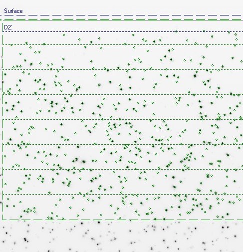 Figure 1. Bulk Micro Defects
Imperfections in the lattice of a semiconductor and impurities create energy states in the bandgap, decrease carrier lifetime, and increase junction leakage. They also act as gettering sites, at which impurities tend to concentrate. The profile of the BMDs is often controlled as shown in Figure 1. by a complex series of high temperature processes to create a “denuded zone”. By this, the surface layer silicon, where the MOS transistor action takes place is free of oxygen precipitates, and the oxygen precipitates in the underlying silicon act as a gettering site to keep impurities away from the MOS transistors.
IR light penetrates most semiconductor materials, and since BMDs alter the local optical properties of a semiconductor, BMDs can be detected by illuminating a sample with IR light and looking at it with a camera that is sensitive to IR.