


Application
EPI RESISTIVITY MEASUREMENT
A blanket layer of silicon can be added to a silicon substrate by a CVD process to achieve changes in the properties, like resistivity, type and defect density. This CVD process is called epi (or epitaxial) deposition. The thickness monitoring of the epi layer is part of the production process of making the epi wafers. This monitoring is executed on a sample basis, or only to confirm that the epi reactor is set up properly.
Semilab can offer non-contact optical solution for Epi thickness monitoring, depending on infrared reflection techniques.
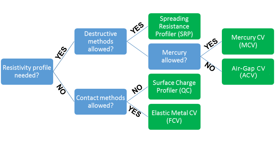 Figure 1. Resistivity measurement flow
Technology
AIR-GAP CV PROFILING
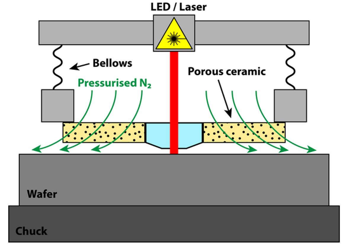 Figure 2. Air-Gap CV profiling
The Air-Gap CV (ACV) technology provides non-contact measurements for epi layers, or substrate resistivity that lowers cost by eliminating test wafer scrap associated with the traditional means of monitoring this specification. All types of the epi substrate can be monitored: p/p+, n/n+, p/p-, n/n+/p+, bare n or n surface.
ACV is conceptually similar to conventional Hg-probe CV or Schottky-CV techniques. The depletion width is determined by applying different voltages at the wafer surface and measuring the resulting capacitance. An air bearing is used to position the sensor very near to the wafer surface without touching. This non-destructive and non-contaminating nature of the method makes it possible to perform reliable measurements on fresh actual product wafers.
An integrated surface treatment chamber (PTC) is used to stabilize the wafer surface after the epi process by creating a uniform, electrically well-behaving native oxide layer.
Ozone (O3) is created by shining UV light into CDA
The wafer is exposed to O3 at elevated temperature (450-490 °C)
Result is a passivated, thus an electrically “well-behaved” native oxide:
- Low charge, Low interface states, homogenous native oxide
PTC process does not affect the wafer characteristics in any way
For fresh wafers, the treatment stabilizes the surface
For old wafers, PTC improves the surface native oxide
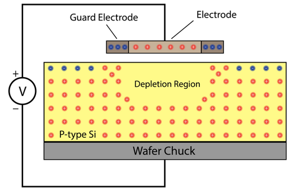 Figure 3. Air-Gap CV
FEATURES
- Non-contact resistivity profiling on product wafers
- Applicable on wide range of n- and p-type samples and all crystal orientations
- ACV profiles may detect problems in epi reactors caused by improper operation
- ACV easily correlates with Hg-CV and other methods
- Independent of buried patterns and buried layers
- Based on classical CV theory
- Eliminates costs of monitor wafers by non-destructive measurements on product wafers
- Faster return of reactor capacity to production
- Increases reactor capacity by decreasing downtime during setup
Product Line
ACV
ACV delivers the industry’s first realtime, non-contact method to measure epi layer resistivity profiles in production. Fast feedback and the availability of the resistivity profile plots and wafer maps aid in troubleshooting for still higher control over epi processes.
100% non-contact, non-destructive measurements of epi layer resistivity by patented technology.
Applications:
- Resistivity and doping concentration depth profile determination in semiconductor epitaxial layers
- Process monitoring
- EPI reactor adjustment
Products

ACV-2200, ACV-3000, ACV-3100 Non-contact Resistivity Profiling Systems
The ACV systems provide 100% non-contact, non-destructive measurements for epi layer resistivity by patented technology. The physics behind the measurement is quite similar to Schottky-CV or Hg-probe, and thus the output is a traditional CV doping profile. The difference is that the electrode does not touch the wafer, resulting in substantial cost savings of monitor wafers.
The model includes complete automation, powerful software and excellent measurement repeatability.
Features and System specifications:
- Number of measurement points, measurement area: No limit in measurement points
- Profile measurement depth: Like MOS CV, depth depends on resistivity and surface charge
- Measurement of all Epi substrate types: p/p+, n/n+, p/p-, n/n+/p+, bare n or p surface. Other structures like p/n or n/p are possible based on pre-sales demo.
| ACV-2200 | ACV-3000 | ACV-3100 | |
|---|---|---|---|
| Wafer Size | 100 to 200 mm | 300 mm | 200 and 300 mm |
| End Effector | Paddle | Edge Grip | Paddle |
| Loadport | Open Casette / SMIF | FOUP | FOUP / SMIF / Open casette |
| Number of Loadports | 1 | 1 or 2 | 1 or 2 |
| Factory Automation | SECS/GEM | Full | Full |
Request Info